Purpose
The RT7273 features three synchronous wide input range high efficiency Buck converters. The converters are designed to simplify its application while giving the designer the option to optimize their usage according to the target application. This document explains the function and use of the RT7273 evaluation board (EVB), and provides information to enable operation, modification of the evaluation board and circuit to suit individual requirements.
Introduction
General Product Information
The RT7273 features three synchronous wide input range high efficiency Buck converters. The converters are designed to simplify its application while giving the designer the option to optimize their usage according to the target application. The converters can operate in 5V, 9V or 12V systems and have integrated power transistors. The output voltage can be set externally using a resistor divider to any value between 0.8V and the input supply minus 1V. Each converter features an enable pin that allows a delayed start-up for sequencing purposes, a soft-start pin that allows adjustable soft-start time by choosing the softstart capacitor, and a current limit pin (RLIMx) to adjust current limit by selecting an external resistor. The COMP pin allows optimizing transient versus dc accuracy response with a simple RC compensation. The switching frequency of the converters can either be set with an external resistor connected to ROSC pin or be synchronized to an external clock connected to SYNC pin if needed. The switching converters are designed to operate from 300kHz to 2.2MHz. The converters operate with 180° phase between CH 1 and CH 2, CH 3 (CH 2 and CH 3 ran in phase) to minimize the input filter requirements. The RT7273 also features a low power mode enabled by an external signal, which allows for a reduction on the input power supplied to the system when the host processor is in stand-by (low activity) mode.
Product Feature
-
Wide Input Supply Voltage Range : 4.5V to 18V
-
Output Range : 0.8V to (VIN - 1V)
-
Fully Integrated Triple-Buck
►Maximum Current 3.5A/2.5A/2.5A
►Continuous Operation 3A/2A/2A
-
High Efficiency
-
Switching Frequency
►300kHz to 2.2MHz Set by External Resistor
-
External Synchronization Pin for Oscillator
-
External Enable/Sequencing Pins
-
Adjustable Cycle-By-Cycle Current Limit Set by External Resistor
-
Soft-Start
-
Current Mode Control with Simple Compensation Circuit
-
Power Good Indicator
-
Discontinuous Operating Mode at Light Load when LOWP = High
Key Performance Summary Table
|
Key Features
|
Evaluation Board Number : PCB068_V1
|
|
Input Voltage Range
|
4.5V to 18V
|
|
Max Output Current (CH1/CH2/CH3)
|
3.5A/2.5A/2.5A
|
|
Default Output Voltage (CH1/CH2/CH3)
|
1.2V/1.8V/3.3V
|
|
Default Marking & Package Type
|
RT7273GQW, WQFN-40L 6x6
|
|
Operation Frequency
|
Set by resistor connected with ROSC pin, with 383kΩ setting for 500kHz switching frequency.
|
Bench Test Setup Conditions
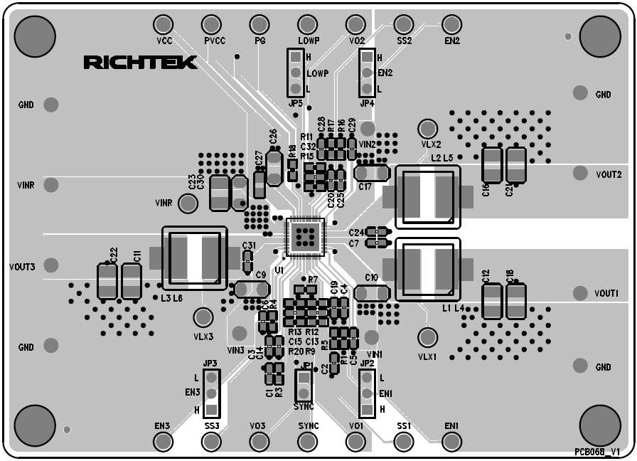
Headers Description and Placement
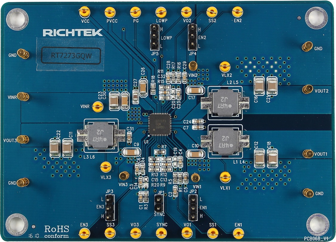
Please carefully inspect the EVB IC and external components, comparing them to the following Bill of Materials, to ensure that all components are installed and undamaged. If any components are missing or damaged during transportation, please contact the distributor or send e-mail to evb_service@richtek.com.
Test Points
The EVB is provided with the test points and pin names listed in the table below.
|
Test point/
Pin name
|
Signal
|
Comment (expected waveforms or voltage levels on test points)
|
|
VIN
|
Input voltage
|
Power input.
|
|
EN
|
Enable test point
|
Externally pulled high to enable and pulled low to disable this chip. It is internally pulled up to high when the pin is floating.
|
|
GND
|
Ground
|
The exposed pad must be soldered to a large PCB and connected to GND for maximum power dissipation.
|
|
VINR
|
Internal Control Circuit Power
|
Supply Voltage Input for Internal Control Circuit.
|
|
PVCC
|
5V Internal Regulator Output
|
Connect a capacitor 10µF between this pin and GND.
|
|
VCC
|
4.6V Internal Regulator Output
|
Connect a capacitor 3.3µF between this pin and GND.
|
|
SS
|
Soft-Start Control
|
Connect an external capacitor between this pin and GND to set the soft-start time.
|
|
PG
|
Power good test point
|
Output of power good indicator.
|
|
LOWP
|
Discontinuous Operation Mode Input
|
Discontinuous Operating Mode at Light Load when LOWP = High (Active High).
|
|
VLX
|
Switch node test point
|
Switch Output for CH 1/2/3.
|
|
SYNC
|
Synchronous Clock Input
|
Connect to GND if not used.
|
Power-up & Measurement Procedure
1. Apply a 12V nominal input power supply (4.5< VIN < 18V) to the VIN and GND terminals.
2. Set the jumper at JP2/JP3/JP4 to connect terminals to H pin, connecting EN to enable operation.
3. Set the jumper at JP1 to short with GND, disable the frequency synchronous function.
4. Verify the output voltage (VOUT1 = 1.2V, VOUT2 = 1.8V, VOUT3 = 3.3V).
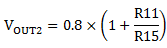
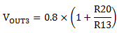
Output Voltage Setting
Set the output voltage with the resistive divider between VOUT and GND with the midpoint connected to FB. The output is set by the following formula :

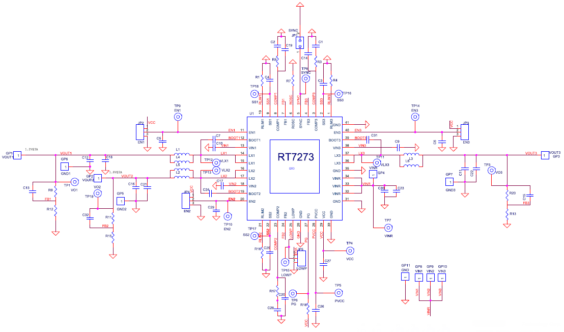
Schematic, Bill of Materials & Board Layout
EVB Schematic Diagram
Bill of Materials
|
Reference
|
Qty
|
Part Number
|
Description
|
Package
|
Manufacture
|
|
U1
|
1
|
RT7273GQW
|
DC/DC Converter
|
WQFN-40L 6x6
|
RICHTEK
|
|
C1, C2, C3, C4, C5, C6, C25, C28, C29
|
9
|
0603B472K500
|
4.7nF/50V/X7R
|
C0603
|
WALSIN
|
|
C7, C24, C31
|
3
|
C1608X7R1H104KT000N
|
0.1µF/50V/X7R
|
C0603
|
TDK
|
|
C9, C10, C17, C26, C30
|
5
|
GRM31CR71E106KA12L
|
10µF/25V/X7R
|
C-1206
|
muRata
|
|
C11, C12, C16, C18, C21, C22, C23
|
7
|
GRM32ER61C226KE20L
|
22µF/16V/X5R
|
C-1210
|
muRata
|
|
C13, C15, C32
|
3
|
0603B471K200
|
470pF/50V/X7R
|
C0603
|
WALSIN
|
|
C14, C19, C20
|
3
|
|
NC
|
C0603
|
|
|
C27
|
1
|
C2012X5R1A335KT000N
|
3.3µF/10V/X5R
|
C-0805
|
TDK
|
|
L1, L2, L3
|
3
|
NR8040T4R7N
|
4.7µH/4.1A
|
8 x 8 x 4 mm
|
TAIYO YUDEN
|
|
R1
|
1
|
|
51k
|
R-0603
|
|
|
R3, R5, R17
|
3
|
|
20k
|
R-0603
|
|
|
R4
|
1
|
|
82k
|
R-0603
|
|
|
R7
|
1
|
|
383k
|
R-0603
|
|
|
R9, R11, R20
|
3
|
|
40.2k
|
R-0603
|
|
|
R12
|
1
|
|
80.8k
|
R-0603
|
|
|
R13
|
1
|
|
12.7k
|
R-0603
|
|
|
R15
|
1
|
|
32.4k
|
R-0603
|
|
|
R16
|
1
|
|
75k
|
R-0603
|
|
|
R18
|
1
|
|
100k
|
R-0603
|
|
|
R1
|
1
|
|
51k
|
R-0603
|
|
|
R3, R5, R17
|
3
|
|
20k
|
R-0603
|
|
PCB Layout
Top View (1st layer)
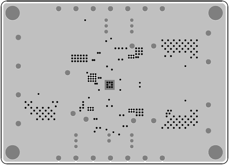
PCB Layout—Inner Side (2nd Layer)
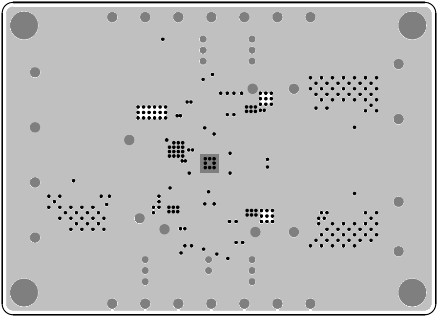
PCB Layout—Inner Side (3rd Layer)
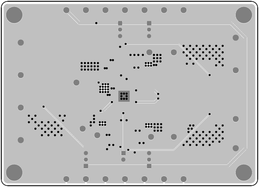
Bottom View (4th Layer)